


A formulation of methylammounium iodide (MAI), PbCl2 and PbI2 at a molar ratio of 1:1:4 (PbCl2:PbI2:MAI) in a DMF solvent. On processing, I201 ink can be used to create a CH3NH3PbI3-xClx perovskite film. The process recipe for I201 is optimised for glove box processing under a nitrogen atmosphere.
I201 perovskite ink is divided into 10 lots of 0.5 ml. We have found this quantity to be sufficient for 10 individual experiments (approximately 160 device substrates).
Datasheet
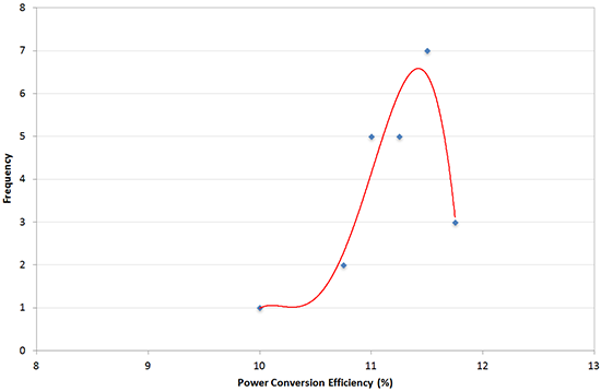
We have specially formulated I201 Perovskite Ink in our laboratories to make it suitable for deposition by spin-coating. It is based on similar ink formulations used in references [1]. This ink is designed to be used with a bottom ITO/PEDOT:PSS anode and a top PC70BM/Ca/Al cathode, with PV devices fabricated with an average / peak power conversion efficiency (PCE) of (11.2% ± 0.4)% / 11.8%. This performance level is in accord with other literature reports using similar ink formulations where PCEs of approximately 11.5% have been demonstrated [1]. A full process recipe comes with the ink, which is ready to use after heating for a short time.

References (please note that Ossila has no formal connection to any of the authors or institutions in these references):
- Reproducible One-Step Fabrication of Compact MAPbI3-xClx Thin Films Derived from Mixed-Lead-Halide Precursors, D. Wang et al., Chem. Mater., 26, 7145-7150 (2014) DOI: 10.1021/cm5037869
Specifications
Perovskite precursor ink formulation: Ink I201 is based on a mixture of methylammonium iodide (MAI), lead chloride (PbCl2) and lead iodide (PbI2) at a molar ratio (PbCl2:PbI2:MAI) of 1:1:4 dissolved in anhydrous DMF (dimethylformamide).
| Compound | Purity | Molar Ratio |
|---|---|---|
| MAI | > 99% (as measured by Elemental Analysis) | 1 |
| PbCl2 | 99.999% | 1 |
| PbI2 | 99.999% | 4 |
| DMF | 99.8% | n/a |
Now selling bulk orders of 30ml with a 25% discount over our standard order sizes.

Usage Details
Fabrication Routine for Perovskite Precursor Ink I201
Glass / ITO / PEDOT:PSS / CH3NH3PbI3-xClx / PC70BM / Ca / Al
For complete step-by-step instructions please see our Full Perovskite Solar Cells Fabrication Video or written fabrication guide. Please note, however, that the routine in these full guides differs slightly to the optimised routine for the I201, which is designed to be processed in a nitrogen filled glove box.
The summary below outlines the key steps required when processing I201 ink. You can also download this summary as a PDF in order to print and laminate it for us in a clean room.
1. Substrate clean (in air):
- Sonicate ITO substrates for 5 minutes in hot (70°C) 1% Hellmanex
- Dump-rinse substrates twice in boiling, deionised (DI) water
- Sonicate for 5 mins in IPA. Dump-rinse twice in boiling DI water
- Dry the substrates with nitrogen gun
- Bake the substrates on a hotplate at 120°C.
2. PEDOT:PSS anode preparation (in air):
- Filter AI 4083 PEDOT:PSS using a 0.45 µm PES filter
- Dispense 35 µl of the filtered PEDOT:PSS solution onto the heated ITO substrate spinning at 6000 rpm for 30s
- Place substrate onto a hotplate at 120°C
- After all ITO substrates have been coated with a PEDOT:PSS layer, transfer all to a nitrogen-filled glove box and place onto a hotplate at 120°C for 20-30 mins
- Remove the substrates from the hotplate and allow to cool at room temperature.
3. Perovskite deposition (in nitrogen glove box):
- Heat I201 ink for 2 hours at 70°C and then cool to room temperature
- Place the ITO coated substrate (at room temperature) onto the spin-coater and spin the substrate at 4000 rpm (for 30s)
- Dynamically dispense 30 µl of I201 ink
- Place substrate back onto the hotplate (in the glove box) at 80°C
- Once all substrates have been coated, anneal for 90 mins
- After 90 mins, use a cleaning swab dipped in a small amount of DMF solvent to wipe the cathode stripe clean
- After cleaning, anneal for an addition 20-30 mins at 80°C to remove any residual DMF solvent
- After this time, remove substrates from the hotplate and cool to room temperature.
4. PC70BM deposition (in nitrogen glove box):
- Prepare a solution of PC70BM at 50 mg / ml in chlorobenzene and stir for 3 to 5 hours
- Place perovskite coated substrate onto the spin-coater and spin at 1000 rpm
- Dispense 20 µl of PC70BM solution onto the substrate (while spinning) and spin for a total time of 30s.
5. Cathode deposition:
- Thermally evaporate a calcium/aluminium cathode (5 and 100 nm respectively) through shadow-mask
- Encapsulate devices using a glass coverslip and encapsulation epoxy
- Expose to UV radiation (350 nm) for 30 mins to cure epoxy.
Perovskite Photovoltaic Device Performance
Below are device characteristics for our best pixel fabricated using the I201 fabrication recipe described above.
JV curves demonstrate the hysteresis observed from the device and include device metrics for both forward and reverse sweeps. The pixel presented (from a reverse sweep) had a power conversion efficiency of 11.8%, a Voc of 0.91 V, a FF of 79% and a Jsc of -16.5 mA/cm2.

To the best of our knowledge the technical information provided here is accurate. However, Ossila assume no liability for the accuracy of this information. The values provided here are typical at the time of manufacture and may vary over time and from batch to batch.
Ossila was founded in 2009 by organic electronics research scientists with the aim of providing the components, equipment and materials to enable faster and smarter research and discovery. We have grown a lot since then and are proud to now supply our products to over 1000 different institutions in over 67 countries across the world.
Having spent many years both in industry and academia developing organic and thin film LEDs, photovoltaics and FETs, we know how long it takes to develop a reliable and efficient device fabrication and testing process. As such, we have developed packages of products and services to enable researchers to jump-start their organic electronics or materials research development program.
Our research scientists have significant experience in the processing of materials into LEDs, PVs and FETs, and amongst our team of physicists, chemists and engineers we have a huge collection of knowledge on thin film processing, electronics and characterisation. The vision behind Ossila is to share this experience with academic and industrial researchers alike and to make their research more efficient. By providing products and services that take the hard work out of the device fabrication process, and the equipment to enable accurate, rapid testing, we can free scientists to focus on what they do best - science.
蚂蚁淘(ebiomall)是苏州蚂蚁淘生物科技有限公司旗下的生物医学科研用品跨境直采(平行进口)平台,自营B2B电商。客户在蚂蚁淘搜索全球产品信息,找到合适的产品后在蚂蚁淘下单,然后蚂蚁淘的海外办事处进行跨境采购、运输到中国口岸,最后由蚂蚁淘国内团队清关并发货给客户。
蚂蚁淘提供“正品保障”、“查价工具”、“限时必达”、“近期拼团”、“现货特惠”、“1元拍卖”“抢购秒杀”、“购物有礼”、“万众创业”等服务,致力于优化供需资源匹配,简化采购流程,加快商品流通速度,数据真实可靠,营造健康的生命科学用品在线交易生态圈。
蚂蚁淘特点:
“专业团队”,蚂蚁淘由产品运营和X实验室两个大团队,其中产品运营团队都是长期从事生命科学用品代理销售行业市场营销、推广销售、采购报关、物流仓储、客服顾问方面的专业人才组成,而我们的X实验室团队主要来自一家已上市的医疗器械B2B平台的项目开发团队。
“标准信息”,蚂蚁淘肩负实现生物医疗科研领域资讯及产品信息全球同步的使命,我们的产品信息全面且做标准化处理,涉及数万家全球优质厂方资源以及百万数量级的生命科学用品信息;
“限时必达”,这是蚂蚁淘的又一大“杀手锏”,部分产品蚂蚁淘提供“时必达”服务,客户在蚂蚁淘下单开始,十天内收到货物,每延迟一天,蚂蚁淘赔付货款的5‰;
“正品低价”,蚂蚁淘不生产生命科学用品,我们搭建的是厂方跟客户的桥梁,客户可以在订单详情查看到所有记录,保障货物由从厂方直接发出,同时蚂蚁淘会不断跟各厂方签订合作协议并公示给客户,建立起彼此的信任;同时,蚂蚁淘采用的是全球直采模式,我们承诺我们的价格具有一定的优势;
“查价工具”,蚂蚁淘是一个查价工具,摒弃行业虚假价格诟病,我们平台的所有数据由蚂蚁淘负责维护,信息唯一且真实可靠,客户可以节省询价的宝贵时间,避免不靠谱的报价;
“物流链共享”,蚂蚁淘可与厂方、客户共享自己的仓储、物流、报关等功能模块;
“正规清关”,我们拒绝人肉代购,CIF100%正规报关,提供17%增票,避免法律风险;
“沟通简单”,如果客户在下单方面有任何疑问,可以随时咨询我们的产品顾问,经验丰富的客服团队,一对一贴心服务,订单详情在线可查,省心省力;
“万众创业”,创业有我,助力梦想起航。“大众创业,万众创新”大浪潮来袭!创业正当时!想加入创业大军的你,在没经验,没方向,没技术,没资源等现实面前停止了创业梦?快来加入蚂蚁淘在校创业合伙人团队,我们找的就是你!
借助互联网平等而开放的力量,矢志实现生命科学领域全球的信息同步与标准化,简化科学家的采购流程,节省科学家宝贵时间。我们相信一群充满梦想的人,可以凭借着专业与执着,让您的购物更轻松!

(蚂蚁淘启动仪式)

(蚂蚁淘徽杭古道自由行)
LOGO诠释

蚂蚁淘的Logo是一个箱子的正视和俯视组成的类三维图,箱子可以包含蚂蚁表达的含义,即运输。E是蚂蚁的首字母(emmet),是ebiomall的首字母,更重要的是E有其他更多的符合我们理念的含义;
1、真实直率(Explicit)
2、极速(Express)
3、轻松购(Easypurchase)
4、高效的(Efficient)
5、电子商务(ElectronicCommerce)
大事记


![]()
暂无问答


本网站将在规定时间内给予删除等相关处理。